-

- /Collaborator
Initiatives for collaboration and contribution
Industry-academia-government collaboration: Joint research with companies,Mutual cooperation with universities,Researcher exchange,ICT research base
Collaborator
Effort
-
-
Collaboration with Industry and Academia
The Advanced ICT Research Institute promotes research & development and social application of the findings as a base of collaboration with Industry, Academia, and Government in advanced and multidisciplinary research fields.
- Joint Research
- We have entered into cooperative agreements with universities to promote research and development, personnel exchanges, student acceptance.
- Human Resource Development
- We cooperate with SSH designated school activities and develop human resources. In some cases, we also exchange memoranda with neighboring high schools.
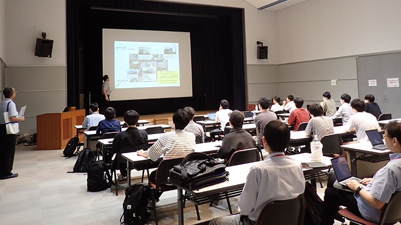
- Facility Tour
- As part of our outreach activities, we accept facility tours.
-
Contribution to the Regional Community
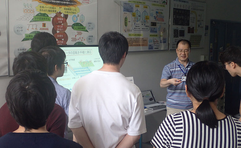
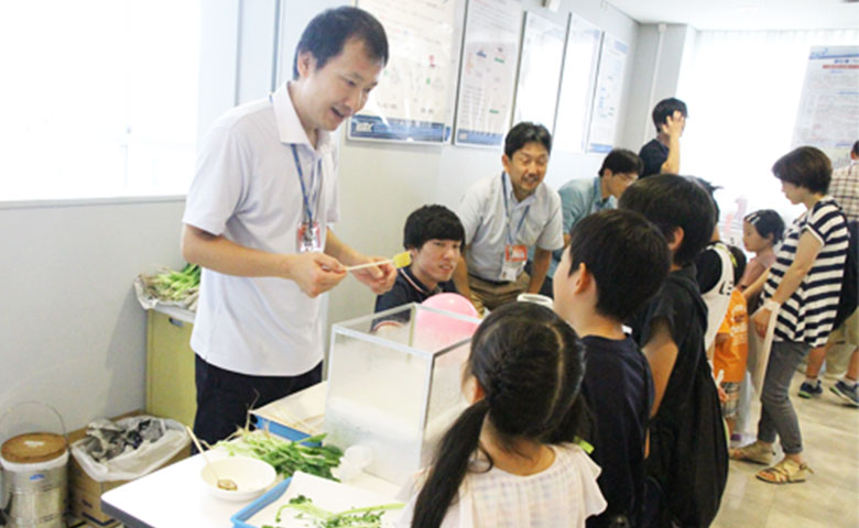
- NICT Open House in Kobe
-
Our institute holds an open house at the end of July every year.
There are various hands-on exhibits which was provided by our researchers so that it can be enjoyed from children to adults.
At the same time, we hold the lecture for the public.
The researcher explains their latest research results easily with familiar example.
There are a lot of visitors every year and it is an important event for get to know our activities.
-
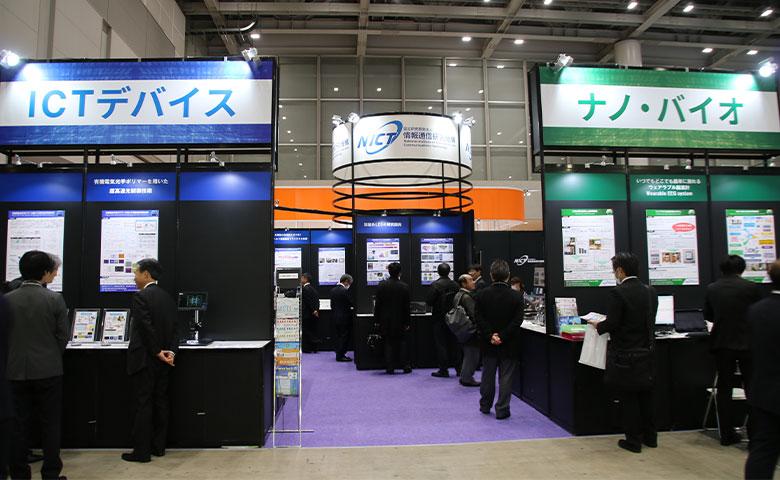
- Exhibitions
-
We have actively participated in exhibitions as a good opportunity to introduce the advanced studies of this institute.
At the same time, we publicize the results that can be introduced to society, such as intellectual property and technology transfer.
The exhibitions provide an opportunity to learn about the needs of society and a good chance for basic researchers to examine the direction of their research.
- International Nanotechnology Exhibition and Conference
- The Kobe International Industrial Fair
- Keihanna information and communications fair
- Hyogo Science Fair
Relevant Departments
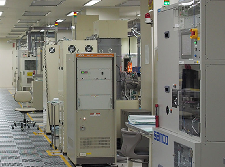
Processing equipments in the clean room
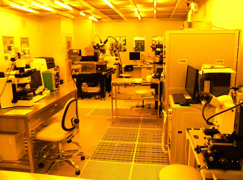
Photo-lithography equipments in the clean room with yellow lights
Kobe Clean Room
Facilities to fabricate nano-devices in the Kobe Clean Room
-
Advanced ICT Device R&D Promotion Center
- [ Background & Policy ]
- Further development and advancement of information and communication technology (ICT) is indispensable to realize wealthy world where all people and things are connected to the network, large-capacity content is freely available, and people live safely based on a wide variety of information. To realize such a future requires fundamental research and development are important, such as cutting-edge optical device technology, millimeter wave/THz wave and other high-frequency technologies, optical/frequency fusion technology, and the exploration of new functional materials, is essential. In these decades, selection and concentration of R&D resulted in the shrink of investments for cutting-edge research and development of challenging device developments, especially in industry. This is primarily because investment for such research is usually based on a medium to long-term perspective and involves high risk, leading to uncertainty regarding future technological development capabilities. NICT as a neutral and highly public research institute, believes it is important to open our Advanced ICT Device R&D Promotion Center ratory. to the public as a research base, and to establish a strong collaboration to promote valuable establishment by research and development with industry and academia. In order to ensure that researchers coming from both domestic and international can effectively utilize our Advanced ICT Device R&D Promotion Center ratory, we will continually improve the operation of the facilities and equipment.
- [ Outline of the Center ]
- Teams of experienced engineers and relevant internal research groups at NICT coordinate with each other to appropriately manage the facility so that users can enjoy a stable and safe work environment that meets standard requirements. Research and development at NICT encompasses the entire spectrum of ICT technologies, featuring the promotion of research on fundamental device technologies with an emphasis on the development of sophisticated information and communication systems at the Advanced ICT Device R&D Promotion Center ratory.
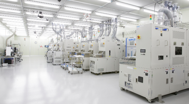
- Advanced ICT Device R&D Promotion Center, Kobe Branch
- The Kobe Cleanroom has been established to promote R&D on Advanced ICT Devices in the western Japan Region. It has been operated in association with the Cleanroom facility at NICT headquarters located in Tokyo. In March 2024, Kobe Device Collaborative Creation Building was newly established to strengthen the collaboration between industry, government, and academia. In order to create next -generation ICT, these facilities have been equipped with a variety of devices required to create superconducting materials and organic nanomaterials as well as to evaluate the characteristics of thin films and devices. More specifically, the following devices have been used in the laboratory: - a load-lock type vacuum film-forming device that is capable of fabricating devices with multiple layer structures; - an atomic layer deposition device that can control film thickness at the atomic scale; - an electron beam lithography system that can draw using a minimum line width of tens of nanometers; - a reactive ion etcher that performs etching on the nanometer scale; and - an inductively coupled plasma (ICP) etcher. As a central hub for the ICT device research, promoting collaboration between industry, government, and academia in the western Japan region, the Kobe Device Collaboration Creation Building provides a one stop environment for evaluating a series of device processes and basic properties. With the recent advances in ICT technology, device research is increasingly dependent on fabrication and measurement using more advanced technologies, and it is urgent to improve R&D environment that meets the needs for device technology. Taking maximum advantage of our state-of-the-art facilities, we will continue to develop breakthroughs in ICT.
-
Promoting quantum technology platform by Industry-academia-government collaboration
-
Quantum ICT Collaboration Center
The Quantum ICT Collaboration Center was established in April 2021 with the aim of advancing R & D in the areas of quantum security convergence and satellite quantum communications, as well as leading the construction of a quantum technology platform that integrates quantum computing, quantum communications and cryptography, and quantum measurement and sensing. In cooperation with related research groups within the NICT, we will actively collaborate with other quantum innovation centers, universities, companies, and public organizations in Japan and overseas, and work on everything from basic research to technology verification, open innovation, and human resource development.
In January 2020, Integrated Innovation Strategy Promotion Council of Japan formulated Quantum Technology Innovation Strategy. This strategy aims to create a quantum innovation hub in Japan that will bring together excellent researchers and engineers from Japan and abroad, attract active investment from companies, and build an organic collaboration and cooperation system between universities and companies.
NICT has also been selected as the Quantum Security Innovation Hub, one of the eight quantum innovation hubs in Japan. The Quantum ICT Collaboration Center will serve as the core organization of the hub in NICT.
-
-
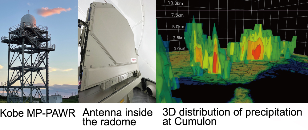
"MP-PAWR"
Remote Sensing Laboratory,
Radio Research InstituteThe latest weather radar, MP-PAWR (Multi-Parameter Phased Array Weather Radar), can observe the rapid development of cumulonimbus clouds that cause localized heavy rain and their signs with high spatial and temporal resolution. Two MP-PAWRs installed at the Advanced ICT Research Institute and at Osaka University Suita Campus are conducting network observations in the Kansai region. The four-dimensional (three-dimensionl space and time) distribution of observed precipitation is publicly available on the web (https://cumulon.jp/).
-
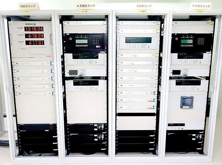
Time measurement system
-
"Kobe substation for Japan Standard Time system"
Space-Time Standards Laboratory,
Electromagnetic Advanced and Infrastructure Research Center,
Radio Research InstituteNICT generates national frequency standards and Japan Standard Time (JST) and also disseminates them throughout Japan. Until 2016, the ensemble of atomic clocks as a basis of the reference time scale for JST was operated exclusively at NICT headquarters in Tokyo. To enhance the capability, reliability and disaster resilience of JST system, the atomic clocks are now also operated in Kobe. We also operate them for the study of clock ensemble system using the clocks in Tokyo, Kobe and two radio-clock stations.
-
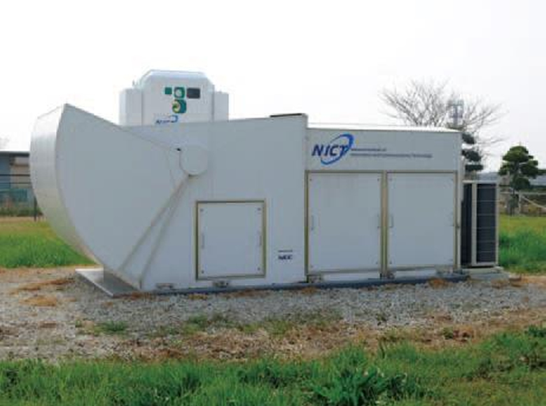
Small Optical Ground Station
-
"Free-Space Optical Communication System"
Space Communication Systems Laboratory,
Wireless Networks Research Center,
Network Research InstituteThis small optical ground station (OGS) for laser communication between satellite and ground was developed in FY2023 as a part of the OGS testbed. A 40 cm telescope is installed in the dome, shown in the figure. The laser beam received by the telescope is precisely tracked at a fixed position (coude focus) relative to the movement of the telescope, and the instruments can be replaced depending on the application. The telescope can also be used to demonstrate site diversity, a method of establishing satellite-to-ground communications in cooperation with other OGS in Japan by selecting locations with favorable conditions.